Showing posts with label using. Show all posts
Showing posts with label using. Show all posts
Thursday, November 21, 2013
Bridge Power Amplifier Using TDA7294
Using TDA7294 audio amplifier integrated circuit in bridge mode configuration , can be designed another Hi-Fi power amplifier .In this TDA7294 bridge power amplifier the value of the load must not be lower than 8 Ohm for dissipation and current capability reasons.
Bridge Power Amplifier Circuit Using TDA7294

The main advantages offered by TDA7294 bridge mode configuration are:High power performances with limited supply voltage level, Considerably high output power even with high load values ( 16 Ohm).The output power of this amplifier in bridge connection is 150 W with Rl= 8 Ohm , Vs = +/-25V the and 170 W output power for Rl=16 Ohm, Vs = +/-35V.
Bridge Power Amplifier Circuit Using TDA7294

Tuesday, November 19, 2013
Battery Charger using LM317 Regulator
 Battery Charger using LM317 Regulator
This Battery Charger is very similar to the universal charger that uses the constant current load. But this is much simpler to build and can be built using only two parties, the LM317 regulator and resistance. The use of diode D is for protection against short circuits. Capacitors C1 and C2 is good voltage regulation. Resistance R2 operates a dummy load when the battery is disconnected. The idea of this magazine is the output current is equal to 1.2 V, divided by the value of R1.
Part List:
LM317
R1 - see the values in table below
R2 - 2.2 kilo-ohms 1/4W
C1,C2 - 47uF/25V, or any value will do, the higher the better
D - 1N4001 or any similar diode at-least 1A rated
Part List:
LM317
R1 - see the values in table below
R2 - 2.2 kilo-ohms 1/4W
C1,C2 - 47uF/25V, or any value will do, the higher the better
D - 1N4001 or any similar diode at-least 1A rated
Simple Metal Detector Using 555 Timer
This metal detector electronic project schematic circuit is designed using a simple 555 timer integrated circuit . As you can see in the schematic circuit , this metal detector electronic project requires few external electronic parts . This circuit detects metal and also magnets.
Metal Detector with 555 Timer Circuit Daigram

When a magnet is brought close to the 10mH choke, the output frequency changes. This metal detector project can be powered from a power supply that can provide an output DC voltage between 6 an 12 volt . If a metal is closer to the L1 coil , will produce a change of output oscillation frequency, that will generate a sound in the 8 ohms speaker
Metal Detector with 555 Timer Circuit Daigram
Saturday, November 16, 2013
Volume Controller Equalizer Using LM1036
This volume controller equalizer electronic project is designed using LM1036 DC tone volume controller with volume and balance circuit for stereo applications .An additional control input of the LM1036 allows loudness compensation to be simply effected.
Volume Controller Equalizer Circuit Using LM1036

The four control inputs of the LM1036 volume controller provides control of the bass, treble, balance and volume functions through application of DC voltages from a remote control system or, alternatively, from four potentiometers which may be biased from a zenner regulated supply provided on the circuit.Each tone response is defined by a single capacitor chosen to give the desired characteristic.
Volume Controller Equalizer Circuit Using LM1036
Wednesday, November 13, 2013
Bidirectional Motor Control Using L293 Driver
Using the L293 quadruple high-current half-H driver integrated circuit can be designed a very simple high efficiency motor control. The L293 is designed to provide bidirectional drive currents of up to 1 A at voltages from 4.5 V to 36 V. The L293D is designed to provide bidirectional drive currents of up to 600-mA at voltages from 4.5 V to 36 V.
Bidirectional Motor Control Circuit Diagram

Each output is a complete totem-pole drive circuit, with a Darlington transistor sink and a pseudo-Darlington source. Drivers are enabled in pairs, with drivers 1 and 2 enabled by 1,2EN and drivers 3 and 4 enabled by 3,4EN. When an enable input is high, the associated drivers are enabled and their outputs are active and in phase with their inputs. When the enable input is low, those drivers are disabled and their outputs are off and in the high-impedance state. With the proper data inputs, each pair of drivers forms a full-H (or bridge) reversible drive suitable for solenoid or motor applications.
External high-speed output clamp diodes should be used for inductive transient suppression. In this bidirectional stepper motor controller electronic project VCC1 is logic supply and must me between 4.5 and 7 volts ( typically 5 volt) and VCC2 is the power supply for the motor and must be from VCC1 up to 36 volts.
Bidirectional Motor Control Circuit Diagram
Each output is a complete totem-pole drive circuit, with a Darlington transistor sink and a pseudo-Darlington source. Drivers are enabled in pairs, with drivers 1 and 2 enabled by 1,2EN and drivers 3 and 4 enabled by 3,4EN. When an enable input is high, the associated drivers are enabled and their outputs are active and in phase with their inputs. When the enable input is low, those drivers are disabled and their outputs are off and in the high-impedance state. With the proper data inputs, each pair of drivers forms a full-H (or bridge) reversible drive suitable for solenoid or motor applications.
External high-speed output clamp diodes should be used for inductive transient suppression. In this bidirectional stepper motor controller electronic project VCC1 is logic supply and must me between 4.5 and 7 volts ( typically 5 volt) and VCC2 is the power supply for the motor and must be from VCC1 up to 36 volts.
Tuesday, November 12, 2013
15W Stereo audio Amplifier using TDA 4935

TDA4935 2x15W audio amplifier is high quality Siemens IC. The IC can be used in stereo or bridge mode. In stereo mode can deliver 15W Stereo audio Amplifier using TDA 4935 per channel in bridge mode can deliver 30W to an 8 ohm load at the source of 30V. TDA4935 requires very few external components and has an ample supply voltage range. The IC operates in class B and has built-in protection circuits over temperature and overload protection.
Notes :
- The circuit must be assembled on a good quality PCB.
- TDA 4935 must be fitted with a proper heat sink.
- The supply voltage can be anything between 8 to 30V DC.
- Capacitors C1, C2, C8 are polyester capacitors.
- Capacitors C3, C4 and C6 are ceramic capacitors while C5 and C9 are electrolytic.
Thursday, October 31, 2013
Ionization Smoke Detector Using A5367
A very simple Ionization Smoke Detector with Interconnect and Timer alarm circuit can be constructed using the A5367 low-current, CMOS circuit that provides all of the required features for an ionization-type smoke detector. A very nice thing at this ionization smoke detector circuit CMOS ic manufactured by Allegro MicroSystems is the interconnection features , which allows as many as 125 units to be interconnected so that if any unit senses smoke all units will sound their alarm. In addition, special features are incorporated to facilitate alignment and test of the finished smoke detector.
This detector needs to be powered by a 9 volts DC power supply (or a 9 volts battery ) .Circuit require few external components and is very easy to be configured . As you can see in this diagram , the sound alarm is “produced “ by an piezoelectric element .
Ionization Smoke Detector Circuit Diagram

Use an external resistor in point A to adjust sensitivity for a particular smoke chamber. Select resistor from point B is to reduce sensitivity during Timer mode.A resistor to VSS or VDD may be added to point C pin to modify low battery voltage threshold. Value of components marked with D will vary, based on the piezoelectric horn used.
An internal timer is provided that can be used in various configurations to allow a period of reduced smoke detector sensitivity, referred to as Timer (or Hush) mode. Internal test circuitry allows low battery check by holding the FEEDBACK and OSC CAP pins low during power-up, then reducing VDD and monitoring the HORN1 pin
This detector needs to be powered by a 9 volts DC power supply (or a 9 volts battery ) .Circuit require few external components and is very easy to be configured . As you can see in this diagram , the sound alarm is “produced “ by an piezoelectric element .
Ionization Smoke Detector Circuit Diagram
An internal timer is provided that can be used in various configurations to allow a period of reduced smoke detector sensitivity, referred to as Timer (or Hush) mode. Internal test circuitry allows low battery check by holding the FEEDBACK and OSC CAP pins low during power-up, then reducing VDD and monitoring the HORN1 pin
Monday, October 28, 2013
Melody Generator using M66T
 Melody Generator using M66T
Components List:
C = 1uF
R = 4.7KW
Q = 2SC9013
About IC M66T series:
The M66T series is a CMOS LSI designed melody generator IC for use in telephones and toys application. It has an on-chip ROM programmed for musical performance. Produced by CMOS technology, the device results in very low power consumption. And with built-in RC oscillator, a compact melody module can be constructed with only a few additional components.

- Pin 1 (O/P) Melody Output
- Pin 2 (Vdd) Positive Power Supply
- Pin 3 (Vss) Negative Power Supply
The following are the M66T series and the song generated by its series:
- M66T-01L : Jingle Bells + Santa Claus Is Coming To Town + We Wish You A Merry Christmas
- M66T-05L : Home Sweet Home
- M66T-09L : Wedding March (Mendelssohn)
- M66T-19L : For Alice
- M66T-68L : It Is A Small World
Sunday, October 27, 2013
32 768 KHz Oscillator using Watch Crystal
 32.768 KHz Oscillator using Watch Crystal
a 32.768 KHz square wave from a common watch crystal. The output can be fed to a 15 stage binary counter to obtain a 1 second square wave. The circuit on the left using the 4069 inverter is recommended over the transistor circuit and produces a better waveform. The single transistor circuit produces more of a ramping waveform but the output swings the full supply voltage range so it will easily drive the input to a CMOS binary counter.
Saturday, October 26, 2013
Stepper Motor Controller Using by A3952S
Using the A3952S stepper motor controller ( designed by Allegro MicroSystems ) we can design a very simple and useful motor driver circuit that can be used in many electronic applications . A3952S stepper motor controller is capable of continuous output currents up to 2 A and operating voltages range up to 50 V. Internal fixed off-time PWM current-control circuitry can be used to regulate the maximum load current to a desired value. The MODE terminal can be used to optimize the performance of the device in microstepping / sinusoidal stepper motor drive applications.
A3952S Stepper Motor Controller Circuit diagram

When the average load current is increasing, slow-decay mode is used to limit the switching losses in the device and iron losses in the motor. The thermal performance in applications with high load currents and/or high duty cycles can be improved by adding external diodes in parallel with the internal diodes. In internal PWM slow-decay applications, only the two top-side (flyback) diodes need be added. For internal fast-decay PWM, or external PHASE or ENABLE input PWM applications, all four external diodes should be added for maximum junction temperature reduction .
As you can see in the schematic diagram , this stepper motor driver circuit require two A3952S circuits and other few additional electronic components.
A3952S Stepper Motor Controller Circuit diagram
As you can see in the schematic diagram , this stepper motor driver circuit require two A3952S circuits and other few additional electronic components.
Sunday, October 20, 2013
Temperature protection using PTC and LM393
Used as a protective circuit above uses a component named PTC , the components in the operating obstacles , but obstacles desert PTC component is influenced by temperature, whereby if the cold temperatures of less than 100 degrees celcius , then this component has a few obstacles. And when temperature run to 100 degrees celcius or higher, which is owned PTC resistance will rise ass well. Because it depends on ambitient temperature , the PTC can be assembled into a circuit protection if high ambitient temperature, tand automatically switchess off, circuit like a schematic above.

R1___4K7
R2___10K
R3___1K9
R4___1M
R5___4k7
TH1__PTC thermistor
IC____LM393
Friday, October 18, 2013
32W Hi Fi Audio Amplifier Using TDA2050
Here is a Hi-Fi power amplifier circuit, built with a power IC TDA2050. This circuit will produce a power output up to 32watt. With good sound quality, high power and very low distortion feature, this circuit will be very suitable for simple and cheap audio systems.
32W Hi-Fi Audio Amplifier Circuit Diagram

TDA2050 Amplifier PCB Design:

About TDA2050:
The TDA 2050 is a monolithic integrated circuit in Pentawatt package, intended for use as an audio class AB audio amplifier. Thanks to its high power capability the TDA2050 is able to provide up to 35W true rms power into 4 ohm load @ THD =10%, VS = ±18V, f = 1KHz and up to 32W into 8ohm load @ THD = 10%, VS = ±22V, f = 1KHz. Moreover, the TDA 2050 delivers typically 50W music power into 4 ohm load over 1 sec at VS=22.5V, f = 1KHz.
The high power and very low harmonic and crossover distortion (THD = 0.05% typ, @ VS = ±22V, PO = 0.1 to 15W, RL=8ohm, f = 100Hz to 15KHz) make the device most suitable for both HiFi and high class TV sets.
32W Hi-Fi Audio Amplifier Circuit Diagram
The TDA 2050 is a monolithic integrated circuit in Pentawatt package, intended for use as an audio class AB audio amplifier. Thanks to its high power capability the TDA2050 is able to provide up to 35W true rms power into 4 ohm load @ THD =10%, VS = ±18V, f = 1KHz and up to 32W into 8ohm load @ THD = 10%, VS = ±22V, f = 1KHz. Moreover, the TDA 2050 delivers typically 50W music power into 4 ohm load over 1 sec at VS=22.5V, f = 1KHz.
The high power and very low harmonic and crossover distortion (THD = 0.05% typ, @ VS = ±22V, PO = 0.1 to 15W, RL=8ohm, f = 100Hz to 15KHz) make the device most suitable for both HiFi and high class TV sets.
Tuesday, October 15, 2013
Fire Alarm using NE555 and temperature sensor

This is a simple series of fire alarms. In this series used NE555 timer and temperature sensor to detect high temperatures. The working principle of this temperature sensor that is when the temperature is high around the sensor then there is resistance on the sensor to be small.
However if the low temperature then the resistance will be high. If the resistance of small sensors, the voltage supply will be able to flow past the sensor and activate the transistor.

IC1 NE555 as a regulator of the audio frequency. Transistors 1 and 2 are used as a driver IC1. Output (pin 3) of IC1 would trigger a transistor base T3 (SL100), which drives the speaker to produce sound the alarm. Frequency NE555 depending on resistance values of R5 and R6 and the capacitance sensor C2 temperature. When the temperature gets hot, would provide a low resistance so that supply voltage can flow into the base of transistor T1 through a diode D1 and R2.
Capacitor C1 will charge a positive voltage so that it will increase the time when the fire alarm. The greater the value of C1, the greater the positive bias applied to the base of transistor T1 (BC548). T1 collector coupled to the base transistor T2, transistor T2 provides a positive voltage to pin 4 (reset) from IC1 (NE555). Resistors R4 will make IC1 NE555 continued to be active despite no positive voltage flowing.
SW Receiver Using MK414
A Short Wave Receiver based on the MK484 (formerly ZN414) that includes the tropical bands and 49 metre bands.
SW Receiver Using MK414 Circuit Diagram

Notes:
The original data sheet for the MK414 states a maximum working frequency is around 4 MHz. SW transmissions are so powerful that this receiver will work well with signals up to about 6 or 7 MHz. The 10k resistor controls the operating voltage for the IC which is critical for good performance.
Coil Details:
The tuned circuit consists of a variable capacitor and fixed air spaced coil. For the coil, I wound between 10 and 20 turns of wire on an empty tube of around 1.5 inches diameter. The turns were spaced so that the overall length was around 3 inches. The variable capacitor tuned 0 - 300 pF but there is plenty of scope for experiment here. One final point, you will need an external antenna to receive broadcasts. I have an outside wire that is about 7 meters long and this was quite effective. The antenna can be connected at either end of the coil or via a series capacitor value between 10pF and 100pF.
SW Receiver Using MK414 Circuit Diagram
Notes:
The original data sheet for the MK414 states a maximum working frequency is around 4 MHz. SW transmissions are so powerful that this receiver will work well with signals up to about 6 or 7 MHz. The 10k resistor controls the operating voltage for the IC which is critical for good performance.
Coil Details:
The tuned circuit consists of a variable capacitor and fixed air spaced coil. For the coil, I wound between 10 and 20 turns of wire on an empty tube of around 1.5 inches diameter. The turns were spaced so that the overall length was around 3 inches. The variable capacitor tuned 0 - 300 pF but there is plenty of scope for experiment here. One final point, you will need an external antenna to receive broadcasts. I have an outside wire that is about 7 meters long and this was quite effective. The antenna can be connected at either end of the coil or via a series capacitor value between 10pF and 100pF.
Monday, October 7, 2013
LED Torch using NSI45090JDT4G Constant Current Regulator
A very simple LED torch can be designed using the NSI45090JDT4G adjustable constant current regulator (CCR) designed by ON Semiconductor ,using extreme few external components. NSI45090JDT4G device is designed to provide a cost effective solution for regulating current in LEDs. This Constant current regulator is based on patent-pending Self-Biased Transistor (SBT) technology and regulates current over a wide voltage range. It is designed with a negative temperature coefficient to protect LEDs from thermal runaway at extreme voltages and currents.
LED Torch Circuit Diagram

The Radj pin allows Ireg(SS) to be adjusted to higher currents by attaching a resistor between Radj (Pin 3) and the Cathode (Pin 4). The Radj pin can also be left open (No Connect) if no adjustment is required.The maximum current that can be adjusted using this chip is around 160 mA , and the maximum input voltage is around 45 volts The D1 from the circuit shown here is used for reverse battery protection .
Bellow you can see how simple is to design a circuit using this chip ( all data shown bellow are for this schematic ) .
LED’s = ((Vin − QX VF − D1 VF)/LED VF)
Example: Vin = 12 Vdc, QX VF = 3.5 Vdc, D1VF = 0.7 V
LED VF = 2.2 Vdc @ 30 mA
(12 Vdc − 4.2 Vdc)/2.2 Vdc = 3 LEDs in series.
LED Torch Circuit Diagram
The Radj pin allows Ireg(SS) to be adjusted to higher currents by attaching a resistor between Radj (Pin 3) and the Cathode (Pin 4). The Radj pin can also be left open (No Connect) if no adjustment is required.The maximum current that can be adjusted using this chip is around 160 mA , and the maximum input voltage is around 45 volts The D1 from the circuit shown here is used for reverse battery protection .
Bellow you can see how simple is to design a circuit using this chip ( all data shown bellow are for this schematic ) .
LED’s = ((Vin − QX VF − D1 VF)/LED VF)
Example: Vin = 12 Vdc, QX VF = 3.5 Vdc, D1VF = 0.7 V
LED VF = 2.2 Vdc @ 30 mA
(12 Vdc − 4.2 Vdc)/2.2 Vdc = 3 LEDs in series.
Friday, October 4, 2013
Light Level Indicator Using a Window Comparator
The second example below uses a LDR (light dependent resistor) to indicate some desired light level. The LDR has a large dynimic range and varies in resistance from less than 100 ohms on a cloudy day to over a megohm in total darkness. A 2K pot was used to adjust the window range for usual room light conditions. This setup might also be used to indicate sunrise/sunset conditions.
Light Level Indicator Circuit Diagram
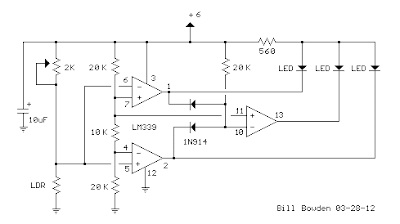
Light Level Indicator Circuit Diagram
Thursday, October 3, 2013
Emergency Lamp using IC 555

Emergency Lamp With 555 is one solution for lighting during power outages. With Emergency Lamp Series 555 uses a 12VDC voltage source that can be supplied from the 12V battery. Emergency Lamp 555 Series With these very simple and easy to make because all the components easily available in the market.
Emergency Lamp Series With this 555 can turn on the light 5W-10W. The circuit is built with an astable multivibrator with the IC 555 that is used to mendrive transformer through Q1. For more details can be viewed directly from the series Emergency Lamp With 555 follows.
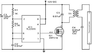 |
| Emergency Lamp Using TLC555 |
Working frequency range of 555 Emergency Lamp With this set of configurations R1, R2 and C2. T1 in series Emergency Lamp With 10V 500mA 555 is a transformer. Secondary part (0-10V) is connected to the Q1 to be given the signal from the multivibrator. Then the primary (0-220V) is connected to the lamp.
Tuesday, September 24, 2013
Metronome Generator Circuit using NE555
 Here is a simple circuit with NE555 IC that can be used to generate metronomes.Such circuit is very useful for those who learn music. The circuit is simply an astable multivibrator NE555 cable around. The components R1, R2 and C1 determine the frequency
Notes.
- The circuit can be wired on a general purpose PCB or common board.
- The circuit can be powered from a 9V PP3 battery.
- The POT R1 can be used to adjust the rhythm of the sound.
- The POT R2 can be used as volume control.
- The speaker k1 can be a n 8 Ohm tweeter.
Thursday, September 19, 2013
Switching Mode Power Supply using STR
 Switching Power supply circuit produces a voltage B + (dc voltage) needed television series taken from the net voltage household. G7 G7A chassis and power supply circuit using cool / cold in which the primary and the secondary power supply electrically separated so that the chassis can be directly connected to another device via an audio video terminal.
 |
| Switching power supply |
This power supply circuit is a type SMPS (Switching Mode Power Supply) using mosfet transistor integrated circuit voltage controller in one IC package, namely STR-W6654. This IC will control the duty cycle of time off Vth2 Mosfet transistor to control the output voltage. Besides, the IC is also equipped with a safety circuit against overvoltage (OVP), overcurrent (OCP) and over temperature (TSD) circuit is working on 220V ac voltage with the input ac voltage range of 176V to 260V ac or known by the Wide range Regulators.
How to Work Series
Initial bias voltage dc pin6 IC801 obtained from an ac voltage through D811 and R817, in the beginning of this pin6 high input impedance, or simply need a current of about 100uA, if the voltage has reached the 10V, the IC will mendrive Mosfet transistor into On and transformer will generate stress induction through V1 , R819 and D816 making this pin6 voltage rises to 16V working voltage, and at this point impedance pin6 will shrink or current will increase to 30mA.
Voltage Stabilizer
Stabilizing the output voltage of the circuit is done by regulating the length of time off of the transistor current MOSFETs by using the feedback coupler photo released by the D807. And the D807 is controlled by the IC regulator IC802, IC is working based on the transformer secondary winding S2 (main output). Change IC802 PIN1 perceived stress will be informed on the photo coupler D807 and forwarded to the IC801 for correction.
Safety Over Voltage
In the event of errors / defects in the feedback path, the output voltage will rise out of control, but the series / IC801 has been equipped with a safety overvoltage, where pin6 IC801 can serve as a detection voltage, output voltage rises when the voltage V1 uncontrolled transformer also rises and via the R819, D816 IC801 pin voltage also rose, When the voltage reaches 34V in IC801 oscillator will stop / off switch and voltage pin6 will go down, and when the voltage reaches 7.5 V IC is going back to work and pin6 voltage rises again, if it again reaches 34V IC will die, so planes demikiian will be dead-alive, dead-alive.
Safety Flow / Cost More
The series is able to secure the power supply circuit to the flow or more load by detecting current flowing in the drain-source transistors MOSFETs. By placing a resistor R809, R835, and R811 on pin3 (source) and connected to pin7 (OCP), the more current or voltage drop on this resistor can be directly detected by a safety circuit overcurrent (OCP). In the event of overload or over current IC will stop for pin 6 voltage above 7.5V
Safety Over Temperature
IC STR-W6654 is also equipped with over temperature safety circuit (TSD). If an error occurs in the IC cooling load or metal, can cause uncontrolled temperature rise IC if IC exceeds 140 degrees then it will stop. The aircraft can live again when the voltage is below 7.5V pin6 (main switch is turned off) and the temperature has dropped below 140 degrees.
Stand-By Condition
With working characteristics pin6 tapped IC STR-W6654 especially voltage Latch Circuit Release Voltage (7.5V) the IC can be made to work on a very small load conditions (stand-by)
How it works series Stand-By
In normal conditions PIN1 UOC IC output is 5V (high) and on stand-by condition 0V (low). If the output of PIN1 UOC Low, Q852 off, Q857 is on, thus the input voltage to 10V PIN2 of IC 802 that will cause the output voltage to 52 volts IC801 PIN1. Thats due to the influence of input voltage PIN1 decreased from 26 V to 10V. so that the circuit feed back will inform you as there is more current. IC 801 IC801 stop temporarily until voltage falls below 7.5V pin6. After reaching 7.5V IC801 automatically revived. So this event will be repeated with certain intervals. The fall in line with all automatic 90V secondary circuit also fell, including PIN1 (V1) transformer. If the transformer voltage drop V1 also fell tentunnya pin6 IC801, IC801 will follow the working characteristics pin6.
In the event of errors / defects in the feedback path, the output voltage will rise out of control, but the series / IC801 has been equipped with a safety overvoltage, where pin6 IC801 can serve as a detection voltage, output voltage rises when the voltage V1 uncontrolled transformer also rises and via the R819, D816 IC801 pin voltage also rose, When the voltage reaches 34V in IC801 oscillator will stop / off switch and voltage pin6 will go down, and when the voltage reaches 7.5 V IC is going back to work and pin6 voltage rises again, if it again reaches 34V IC will die, so planes demikiian will be dead-alive, dead-alive.
Safety Flow / Cost More
The series is able to secure the power supply circuit to the flow or more load by detecting current flowing in the drain-source transistors MOSFETs. By placing a resistor R809, R835, and R811 on pin3 (source) and connected to pin7 (OCP), the more current or voltage drop on this resistor can be directly detected by a safety circuit overcurrent (OCP). In the event of overload or over current IC will stop for pin 6 voltage above 7.5V
Safety Over Temperature
IC STR-W6654 is also equipped with over temperature safety circuit (TSD). If an error occurs in the IC cooling load or metal, can cause uncontrolled temperature rise IC if IC exceeds 140 degrees then it will stop. The aircraft can live again when the voltage is below 7.5V pin6 (main switch is turned off) and the temperature has dropped below 140 degrees.
Stand-By Condition
With working characteristics pin6 tapped IC STR-W6654 especially voltage Latch Circuit Release Voltage (7.5V) the IC can be made to work on a very small load conditions (stand-by)
How it works series Stand-By
In normal conditions PIN1 UOC IC output is 5V (high) and on stand-by condition 0V (low). If the output of PIN1 UOC Low, Q852 off, Q857 is on, thus the input voltage to 10V PIN2 of IC 802 that will cause the output voltage to 52 volts IC801 PIN1. Thats due to the influence of input voltage PIN1 decreased from 26 V to 10V. so that the circuit feed back will inform you as there is more current. IC 801 IC801 stop temporarily until voltage falls below 7.5V pin6. After reaching 7.5V IC801 automatically revived. So this event will be repeated with certain intervals. The fall in line with all automatic 90V secondary circuit also fell, including PIN1 (V1) transformer. If the transformer voltage drop V1 also fell tentunnya pin6 IC801, IC801 will follow the working characteristics pin6.
Monday, September 16, 2013
6 Channel LED Driver Using MCP34845
A very simple 6 channel low cost led driver electronic circuit project can be designed using the MCP34845 LED drivers manufactured by Free scale Semiconductor.The MCP34845 LED drivers operates from 5 to 21 volts and is specially designed for use in back lighting LCD displays from 10" to 17"+ for devices like : PC Notebooks , Net books , Picture Frames , Portable DVD Players , Small Screen Televisions , Industrial Displays , Medical Displays , etc.
6 Channel LED Driver Circuit Diagram
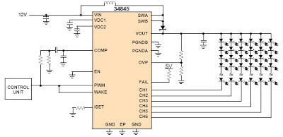
The MCP34845 LED drivers is capable of driving up to 16 LEDs in series in 6 separate strings.PWM dimming is performed by applying a PWM input signal to the PWM pin which modulates the LED channels directly.Main features of this driver circuit project are : input voltage of 5.0 to 21 V , boost output voltage up to 60 V, 2.0 A integrated boost FET , fixed boost frequency - 600 kHz or 1.2 MHz , OTP, OCP, UVLO fault detection , LED short/open protection , programmable LED current between 3.0 mA and 30 mA .
6 Channel LED Driver Circuit Diagram
The MCP34845 LED drivers is capable of driving up to 16 LEDs in series in 6 separate strings.PWM dimming is performed by applying a PWM input signal to the PWM pin which modulates the LED channels directly.Main features of this driver circuit project are : input voltage of 5.0 to 21 V , boost output voltage up to 60 V, 2.0 A integrated boost FET , fixed boost frequency - 600 kHz or 1.2 MHz , OTP, OCP, UVLO fault detection , LED short/open protection , programmable LED current between 3.0 mA and 30 mA .
Subscribe to:
Posts (Atom)