Showing posts with label voltage. Show all posts
Showing posts with label voltage. Show all posts
Sunday, December 15, 2013
0 300V Variable High Voltage Power Supply
Here is the variable high voltage dc power supply circuit, which we can customize the output voltage from 0 to 311Vdc, and it is protected the current over limit that we define at about 100 mA.

In the circuit you can see the T1 is a mains transformer with a ratio of 1:1, for security reasons , and reduces noise signal as well. Then the mains voltage from the T1 is rectified to DCvolt with bridge diode D1-D4, We use a No. 1N4007 that withstand voltage as 1,000V at the current 1A and and this DCV is filtered through the capacitor C1 – 220uF 400V be the big size electrolytic types, by the voltage drop across C1 is about 311VDC.
The power MOSFET Q1 is controlled the current output, with using the resistor R3 – 500K adjust the voltage gate pin of Q1. The ZENER diode ZD1-12V is available prevent over voltage at gate pin of the Q2 if we not has it when high volt the Q2 may be damaged.
The transistor Q2-BC337 and the shunt resistor R2 – 3.3ohm are added for as a current limiter. When the current output is too increased, the Q2 will stop the gate pin of the Q1 immediately, which will be guard the higher current output. The degree of R3 gets from testing in this circuit, which depending on the gain of the transistor or the hFE value, so you may need to tune the value of R2

Saturday, December 14, 2013
Frequency to Voltage Converter Circuit
IC LM2917 Frequency to Voltage Converter
IC LM2917 IC chip is designed specifically as a Frequency to Voltage Converter or Frequency to Voltage converter. In its use to applications Frequency to Voltage Converter IC LM2917 requires few external components.
There are several examples of applications of Frequency to Voltage Converter IC LM2917 datasheet that is included in the LM2917 IC. In this article series Frequency to Voltage Converter IC also taken from the LM2917 datasheet. The advantages of single chip LM2917 Frequency to Voltage Converter is able to provide instantaneous volt output o at time of frequency change 0 Hz. Very easy to apply in measuring the output frequency with the formulation of single-chip Frequency to Voltage Converter VOUT = FIN x VCC x R1 x C1.Then the single-chip LM2917 Frequency to Voltage Converter This configuration requires only the RC only in frequency doubling. And has an internal zener regulator to aimlessly accuracy and stability in frequency-to-voltage conversion process.
Application circuit Figure IC LM2917 as Frequency to Voltage Converter

Feature-owned single-chip LM2917 Frequency to Voltage Converter
Reference to ground directly with variable reluctance
Op Amp / Comparator with transistor output
50 mA maximum output currents for application directly to the load
Frequency doubling for low ripel
Buid in zener
Linear output ± 0.3%
Application single chip LM2917 Frequency to Voltage Converter
Frequency to Voltage Converter
Rotation speed sensor applications
Speedometer
Tachometer
Cruise Control
Cluth Control
And other applications associated with the measurement of rotation speed or frequency measurements.
Friday, November 1, 2013
Voltage Feedback Op Amp
VOLTAGE FEEDBACK OPERATIONAL AMPLIFIER
Device Description:
Voltage feedback operational amplifiers usually manufactured for industrial use have ultra-low power requirements, with a typical quiescent current value of approximately 250 micro amperes. The typical current drawn in powered-down mode for such an amplifier is 0.5 micro amperes. They are suitable for operation at any bandwidth below 56 MHz. The manufacturing process is called a SiGe complimentary bipolar process. It is an advanced method used at the industrial level.
Ultra-low power-op amps have rail-to-rail output along with negative rail input. They are specially designed to operate under an EMF ranging from 2.5 – 5.5 Volts. There are two options: the single or dual supply operational amplifier. The aforementioned voltage supply is for single mode op amps whereas for a dual mode operational amplifier the power supply ranges from -1.25 to -2.25 Volts and 1.25 to 2.75 Volts (in dual supply configuration). These operational amplifiers are leading the industry due to their high power/performance ratio. They consume a mere 250 micro amperes of current on each channel, under a unity gain of 56 MHz.
A voltage feedback operational amplifier is well-suited for portable battery applications in which low power consumption is desired along with good performance. It consumes little power, yet offers high frequency performance. Such operational amplifiers serve as the device with high frequency performance in many battery-powered applications by lowering current consumption. This is achievable on account of a power saving mode, in which its current consumption can be lowered to 1.5 micro amperes. A voltage feedback operational amplifier consists of an integrated gain setting resistor in its both single and dual supply variants. These gain setting resistors are bound to a printed circuit board with the smallest possible size across a wide range of attainable gain values - they can be replaced with a potentiometer for controllable resistance. The design of a voltage feedback operational amplifier impacts the range of attenuation values. These amplifiers are designed to work at industrial-standard temperatures ranging from -40 to 250 degrees centigrade.
Applications of Voltage Feedback Operational Amplifiers
A voltage feedback operational amplifier has many industrial applications, including the following:
• Audio ADC input buffers
• Portable systems
• High density systems
• Low power systems
• Ultrasonic flow systems
• ADC Drivers
• Low power SAR
• Low power signal conditioning systems.
Device Description:
Voltage feedback operational amplifiers usually manufactured for industrial use have ultra-low power requirements, with a typical quiescent current value of approximately 250 micro amperes. The typical current drawn in powered-down mode for such an amplifier is 0.5 micro amperes. They are suitable for operation at any bandwidth below 56 MHz. The manufacturing process is called a SiGe complimentary bipolar process. It is an advanced method used at the industrial level.
Ultra-low power-op amps have rail-to-rail output along with negative rail input. They are specially designed to operate under an EMF ranging from 2.5 – 5.5 Volts. There are two options: the single or dual supply operational amplifier. The aforementioned voltage supply is for single mode op amps whereas for a dual mode operational amplifier the power supply ranges from -1.25 to -2.25 Volts and 1.25 to 2.75 Volts (in dual supply configuration). These operational amplifiers are leading the industry due to their high power/performance ratio. They consume a mere 250 micro amperes of current on each channel, under a unity gain of 56 MHz.
A voltage feedback operational amplifier is well-suited for portable battery applications in which low power consumption is desired along with good performance. It consumes little power, yet offers high frequency performance. Such operational amplifiers serve as the device with high frequency performance in many battery-powered applications by lowering current consumption. This is achievable on account of a power saving mode, in which its current consumption can be lowered to 1.5 micro amperes. A voltage feedback operational amplifier consists of an integrated gain setting resistor in its both single and dual supply variants. These gain setting resistors are bound to a printed circuit board with the smallest possible size across a wide range of attainable gain values - they can be replaced with a potentiometer for controllable resistance. The design of a voltage feedback operational amplifier impacts the range of attenuation values. These amplifiers are designed to work at industrial-standard temperatures ranging from -40 to 250 degrees centigrade.
Applications of Voltage Feedback Operational Amplifiers
A voltage feedback operational amplifier has many industrial applications, including the following:
• Audio ADC input buffers
• Portable systems
• High density systems
• Low power systems
• Ultrasonic flow systems
• ADC Drivers
• Low power SAR
• Low power signal conditioning systems.
Wednesday, October 30, 2013
Simple Source Voltage Protector

Protection of electronic devices with a DC voltage source of voltage source obligatory reversal, especially protection of the source voltage is reversed. The definition of "Protectors Voltage Sources" in this article are the source voltage surge protector circuit which serves to protect the device from the reversal of the voltage source to the appliance electronics.
Source voltage surge protector will expressed in this article are general, so that later in their applications to stay adjusted value of the component with the voltage source needs an electronic appliance. Let us start reviewing Protectors Voltage Source by simple and modest.
 |
| Source voltage protection with 1 diode |
Diodes are used as a protector of the source voltage installation tebaliknya voltage source is installed in series with the input line voltage source electronics devices. Installation of surge protector diode as a voltage source is on the positive line voltage source input device. The function is to drain diode current (voltage source) in one direction only, so that in the event of an upside-down voltage source. then the voltage source is not in the channel (in blocks) to the device. The value of the diode is tailored to the needs of the source voltage of the device itself.
 |
| Source voltage protection with dioda bridge |
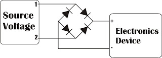
Protectors voltage source with a diode bridge in principle the same as the surge protector with a voltage source diode 1 pc. The difference is the source voltage surge protector is not blocking the source voltage, but the source voltage surge protector is to reverse the flow of the source voltage of one polarity in the case of voltage source. From the picture above to explain the purpose of reversing the voltage source in question, namely when given a source voltage through a voltage surge protector is the source of positive polarity (+) will be directly in the stream leading to the positive input line of tools and the source of negative voltage (-) will be directed to the negative voltage source input line tool.
Monday, October 21, 2013
High voltage inverter circuit diagram

This inverter circuit works with a transistor and transformer and other components to increase the voltage becomes high. Input supply voltage ranging from 3V to 6V DC, later it was raised to high voltage AC. However, in this inverter circuit output current is very small, probably under 0.1A even smaller. However, its use you can apply it on a fluorescent lamp 10W maximum power only, and that too takes time to switch on fluorescent lamps.Part List
R1 = 4K7
R2 = 2K2
R3 = 330K
C1 = 100nF
C2 = 100nF 275V
C3 = 0.22uF 275V
Q1 = D506
L1 = 100 times winding, with 0.8mm diameter copper wire
L2 = 50 times winding, with 0.8mm diameter copper wire
L3 = 5000 times winding, with 0.4mm diameter copper wire
Saturday, October 19, 2013
Voltage to frequency converter

Changing the voltage to frequency scale in the design of an electronic device is sometimes necessary. The series of articles voltage to frequency converter with the XR 4151 is one answer. Voltage to Frequency converter circuit with the XR 4151 is the idea of time in college, when there are projects to create a tool to hatch chicken eggs.
It will be my neighbor also write articles incubators chicken egg-based microcontroller AT89C2051. Maybe there are friends who still remember to this project. Back to the topic of voltage to frequency converter circuit with the XR 4151. IC XR 4151 is a major component of voltage to frequency converter (Voltage to Frequency Converter).
It will be my neighbor also write articles incubators chicken egg-based microcontroller AT89C2051. Maybe there are friends who still remember to this project. Back to the topic of voltage to frequency converter circuit with the XR 4151. IC XR 4151 is a major component of voltage to frequency converter (Voltage to Frequency Converter).

From voltage to frequency converter circuit with XR 4151 on the input signal circuit is a DC voltage level. IC XR4151 on voltage to frequency converter circuit serves to convert the voltage level coming into form in the development of the frequency change, where the output frequency range of voltage to frequency converter with the XR 4151 is proportional to the voltage level input voltage to frequency converter circuit with this 4151 XR.
Sunday, October 13, 2013
Drop Voltage Indicator
An indicator of drop voltage can be achieved using electronic diagram below. This indicator shows the drop voltage or disturbing impulses of any existing network using a LED which will light.
Drop Voltage Indicator Circuit Diagram
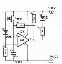
This circuit can be powered with a DC voltage between 5 and 12 volts.
Drop Voltage Indicator Circuit Diagram
This circuit can be powered with a DC voltage between 5 and 12 volts.
Monday, September 30, 2013
7812 voltage stabilizer
 To obtain a pure DC voltage, then we must consider the regulation voltages and currents that we change from AC to DC current. For that we need some settings that can support our own making and its components were easy to get in the electronics market.
This is series Power Supply that can be used on trafo 5 Ampere up to 10 Amperes.

If you want to use a larger transformer than 5 Amperes transistor 2N3055 is suggested that the double for the exit of the collector current is larger and in accordance with the current out of the transformer. How pemasanganya enough in the series on all sides of the pin.
Tuesday, September 24, 2013
Low Voltage Stereo Headphone Amplifier
This is a stereo earphone amplifier circuit of using LM4910 IC. This circuit is very straightforward so it is very cool to comprise even in support of beginners after. for the reason that the voltage source is used solitary 3 VDC you can utilization 2 x A3 battery trendy progression stacking.
 |
| Low Voltage Stereo Headphone Amplifier |
LM4910 Boomer belonging to the series of state Semiconductors is an integrated stereo amplifier is primarily intended representing earphone stereo applications. The IC can come about operated from 3.3V ans its 0.35mW can release output power into a 32 ohm load. The LM4910 has very low distortion (minus than 1%) and the shutdown current is less than 1uA. This low shutdown current makes it as it should be designed for battery operated applications.
C1 and C2 are the input DC decoupling capacitors for the gone and due input channels. R1 and R2 are the respective input resistors. R3 is the feed back resistor representing not here channel while R4 is the feed back resistor for the right channel. C3 is the power supply filter capacitor. The criticism resistors as well sets the blocked ring expansion voguish conjunction with the corresponding input resistors.
Sunday, September 22, 2013
Voltage to frequency converter
Changing the voltage to frequency scale in the design of an electronic device is sometimes necessary. The series of articles voltage to frequency converter with the XR 4151 is one answer. Voltage to Frequency converter circuit with the XR 4151 is the idea of time in college, when there are projects to create a tool to hatch chicken eggs.
It will be my neighbor also write articles incubators chicken egg-based microcontroller AT89C2051. Maybe there are friends who still remember to this project. Back to the topic of voltage to frequency converter circuit with the XR 4151. IC XR 4151 is a major component of voltage to frequency converter (Voltage to Frequency Converter).
It will be my neighbor also write articles incubators chicken egg-based microcontroller AT89C2051. Maybe there are friends who still remember to this project. Back to the topic of voltage to frequency converter circuit with the XR 4151. IC XR 4151 is a major component of voltage to frequency converter (Voltage to Frequency Converter).
From voltage to frequency converter circuit with XR 4151 on the input signal circuit is a DC voltage level. IC XR4151 on voltage to frequency converter circuit serves to convert the voltage level coming into form in the development of the frequency change, where the output frequency range of voltage to frequency converter with the XR 4151 is proportional to the voltage level input voltage to frequency converter circuit with this 4151 XR.
Subscribe to:
Posts (Atom)