Friday, December 20, 2013

Astabil Multivibrator

Multivibrator is a relaxation oscillator type. This circuit uses the RC network and the region contribute to the square wave output. Astabel multivibrator used in the TV receiver to control the electron beam on the picture tube. In this series of computers used to develop the pulse time.


Astabil Multivibrator circuit

HOW TO WORK

A multibrator consists of two cross-coupled amplifier. The amplifier output is one connected to another amplifier wedding. Because each penguata reverse input signal, the combined effect of this is in the form of positive feedback. With the feedback posotif, the oscillator will always get the extra energy (regenerative) and produces a continuous output.

The picture above shows the multivibrator circuit using 2 pieces of bipolar transistors with common emitter configuration. R1 and R2 provide bias voltage developed at the base of each transistor. Holding capacitor C1 to the base collector Q1 Q2. Q2 together with capacitor C2 to the base of Q1.

Because of this cross coupling, a transistor will be conductive and the other is the cutoff. The two transistors alternately will live and die so that the outputs are labeled Q or. That output has a polarity reversal.

When the power given to the multivibrator, one transistor will berkonduksi first, let us assume here that berkonduksi Q1 first. With Q1 berkonduksi voltage on R and Vc decreased, so that its value is lower than VCC. As a result akn happened to the negative voltage on C1 and the positive base voltage of Q1 will decrease. Q2 conduction is reduced and the collector voltage equal to VCC. Voltage will be towards the positive on the C2. This voltage is added to the base of Q1 and make it more berkonduksi. This process continues until reaching saturation point Q1 and Q2 to reach the cutoff.


Multivibrator device functioned as a trigger (triggered device) or free-running. Multivibrator trigger requires the input signal / pulse. Multivibrator output is controlled or synchronized by the input signal.
When the output voltage of each transistor achieve stability, then there is no voltage feedback. Q2 will return berpanjar forward through R2. Conduction in Q2 will lead to a decrease in VC. Voltage to the negative direction will be given on the basis of Q1 through C2. Q1 conduction is reduced. Vc in Q1 will rise worth with Vcc. This will tergandeng to the base of Q2 through C1. This process continues until Q2 Q1 reached saturation point and reach the cutoff. The output voltage then becomes unstable and the process will be repeated.

The frequency of oscillation of the multivibrator time constant distentukan by R2 and R3 and C1 and C2. The R2 and R3 are chosen such that each transistor can reach saturation point. C1 and C2 is selected to obtain the desired operating frequency. If C1 = C2 and R2 = R3 then the output will be symmetrical. Means that both transistors will live and die in selag the same time.
[Continue Reading]

Thursday, December 19, 2013

Power amplifier circuit 60 W mono

Wow this is nice intregated amplifier circuit , because this IC can be power output up to 60 Watt . With minimum require voltage 8 V , and maximum voltage 35 V . But this circuit isnt so good to working on car , because output sound is very loud but not smooth. Amplifier so good working on full range , with speaker full range 100W and impedance 8 Ohm.
Below it is schematic :


Click to view large

The circuit above use IC AN7170 , the original output power IC is 20 W with impedance. But with use the circuit output elevated up to 60W.
[Continue Reading]

Metal Detector Circuit

Metal Detector
One type of metal detector is a type of beat frequency oscillator (BFO). The methods used in metal detectors in general are changing the characteristics of the oscillator when there are close to the metal sensor. The detector works based on the resonant frequency that has been set change when there is a metal object is located quite close to the search coil sensors.


Tuning circuit (tuned circuit) should be a part of our oscillator circuit so that if approached by a metal coil sensor specific hence the output frequency of the oscillation circuit is about to change. Variation changes the output frequency depends on the frequency chosen. The selection of the higher frequency will cause the circuit sensitivity increases because the greater the frequency change. Stay if the selection frequency is too high then the practice will produce a system that is not sensitive. This is because the high frequency of most will not be reflected back but will be absorbed by the soil, building materials.

Metal Detector Circuit

Frequency used (f1-produced by the tank circuit with L1) is usually above the human hearing ability. Because it can not be heard by human pendegaran the frequency changes that occur will also not be heard as well. To overcome this it should be made a separate tone (audible frekuency-f2) which shows the change in frequency. This is said with the beat.

By mixing the two signals (f1 and f2) will produce signals f1, f2, (f1 + f2), and (f1-f2). The signal can be heard by human hearing is a signal (f1-f2). So when there are changes in frequency caused by changes in the characteristics of the search coil can be heard by humans as a rhythm-beat changing. Rhythm-beat is what is the signal (f1-f2) earlier.
VC1 setting is not easy because it requires experiments on certain metals. Similarly, for setting the rhythm of the beat is heard because at a certain condition will feel the rhythm of this beat very disturbing. So it was no possibility the beat or rhythm is not produced beatnya lower than normal because all these conditions can be set on VC1.

So when there are changes in the characteristics of the search coil it will produce sound frequency also depends on the different frequencies generated by the L1 and L2 frequencies generated by.
This method still has the disadvantage that its output frequency variation is still too small to change its frequency is almost not visible. Additionally, on certain conditions Dapa produce a frequency below the audible sound. For that we need a reconfiguration of coupling capacitors and the frequency of use.
The values ​​of existing components dirangkaian Figure 2 represents the values ​​specified in a metal. So for a specific metal component values ​​need to be adjusted especially VC1, C1, C4, and C5.

Inductor L1 is formed from the coil that serves as a search coil. This inductor will resonate along with the VC1 to produce a tank circuit with Q high. The second oscillator is formed from L2, C4, C5, R4, and Q2 and the oscillator circuit will produce a signal with a fixed frequency. D1 serves as a simple mixing between f1 and f2 and will generate a signal with a frequency (f1-f2) and a lot of harmonic signals. Signal with a frequency (f1-f2) is made so that it can be in areas that can be heard by human hearing.

Suppose that f1 and f2 on the 100KHz 101KHz then after dimixer, signal (f1-f2) will produce a signal with a frequency of 1kHz. This differential signal must be amplified in advance using a opamp that will only be able to drive headphones with high impedance. If the chill to be used for regular headphones then Dapa LM741 amplifier chip is replaced with the type of audio amplifiers. Because ampilifier audio output has a low impedance. Amplifier gain setting is determined from the setting R7 and R10, and if necessary the output of the LM741 can be incorporated into a power amplifier circuit to drive an spaker.

Circuit in Figure 2 is very simple to allow the occurrence of frequency drift - a shift in frequency. This is usually caused by the temperature factor. However this problem is not a serious problem. Permsalahan can ditanganni by searching for capacitor components which have a large enough temperature tolerance. In addition, PCB layout also has a huge effect on this problem.

The size of the search coil depends on the sensitivity of metal detectors are cooled and form of the sensor itself. For example, a large search coil which of course can easily find the metal you are looking at a large area rather than a metal detector with a small search coil. Instead of metal detectors can not determine the location of cables on a wall tertanan precisely because of the large size of the sensor.

So the greater the search coil, the accuracy of his smaller but bigger sensitivty but instead a small search coil, commonly used to compact metal detector, have high accuracy but less sensitivity. The shape of the search coil is usually a circle or square. Besides needing a shield layer which serves to reduce electrostatic effects and effects caused by capacitive objects.
[Continue Reading]

Low battery detector circuit

You feel confused to detect wether a battery is low or high, or you want to be notified if the battery and has expired , this circuit can detect if a battery has begun to decrease its strength. Circuit is based on LM4250 IC is able to detect if the battery runs out and will issue a notification signal.
[Continue Reading]

Wednesday, December 18, 2013

Toggle Switch with IR

Toggle switch in this article is a series of toggle switches that are controlled by infrared light. The series toggle switch is made from a combination of data flip-flop CD4013 2 units. Receiver circuit of the infrared light signals arranged with infrared receiver as found on television remote receiver. Infrared signal from remote is used as clock signals and data to the data flip-flop first. then the second flip-flop data set as a toggle flip-flop toggle the output signal is used to drive the relay. for more details can be seen in thethe following image .


Toggle switch with Infra Red IR


Series Toggle Switch With Infra Red (IR) that is required to supply voltage range of 12VDC and the output of Toggle Switch With Infra Red (IR) is dapt used to turn on the lights or other electronic devices with DC or AC voltage source. Series Toggle Switch With Infra Red (IR) was isolated from the load that is placed for use as the final relay.


source [link] 
[Continue Reading]

ADC 0804 Microcontroler Interface Engineering

Microcontroller Interface Engineering With ADC 0804
In ADC 0804 interface techniques with microcontrollers are pin-pin control must be controlled if we want to use the ADC with the microcontroller, there is value addition refferensi voltage to be supplied in 0804 ADC interface with a microcontroller, for example, we use the 0804 ADC (8 bit), if we give refferensi voltage 2.55 volts then we will get the increase of 1 bit to change 10 mVolt. Please note that the 0804 ADC pin on the leg that is form Vref Vref / 2, so to get a 10mV resolution is necessary for setting Vref / 2 equal to 1.275 V


The interface circuit microcontroller with ADC 0804


Mechanical interface microcontroller with ADC 0804
The steps in accessing data from the ADC 0804 by the microcontroller sebgai follows;

Enable ADC with signal 0 at the foot of Chip Select.
Give commands from conversion by providing a low pulse to the foot of the ADC Write narrow
Wait for the ADC issued a signal 0 from his leg INT
Give a moment of time delay for data from the ADC is correct
Give the read command by giving the signal 0 at the foot of ADC Read
Give a moment of time delay
Now data from the ADC is ready for use and if the microcontroller.
[Continue Reading]

Schematic Power Amplifier with IC AN7117

 *notif : this circuit is mono amplifier

Anyone who uses this amplifier circuit would be surprised. Although this circuit has a small power output just 10 watts , but also issued a sound loud enough. At least match the transistor power amplifier with 60 watts. And his sound is good with low noise. Minimum voltage is 2 volt , and maximum voltage is 12 volt .

Schematic circuit power amplifier AN7117 below :


Click image to view Enlarge
[Continue Reading]

Auto Sound Systems One Piece at a Time

Those who are in the market for auto sound systems are probably well aware of the many decisions that need to be made throughout the process. Gone are the days when you went in, pointed to a box and walked out with all the pieces, parts, and components you would ever need for a really kickin sound. The truth of the matter is that there are many pieces and parts that work together in order to create the ultimate sound system and everyone seems to have different requirements, styles, tastes, and budgets to work with.
Because of this, many manufacturers of auto sound systems have wised up to the fact that some people will buy the components they need to create the sound system of their dreams piece by piece as budgets allow. This is actually a very intelligent way for customers on a budget to buy the sound system they are hoping to some day have. As a result you will find that speakers, amplifiers, sub woofers, and the actual stereo are often sold separately and at very reasonable prices.


Most of us hate living within limited budgets but understand that often in life it is a necessary evil. Living on a budget is not such a terrible thing really. If we had everything we wanted, what on earth would there be to look forward to? At least that is what I keep telling myself. I, however, seem to be the queen of budget living and bargain hunting. I love little more in life than finding a great deal on an item Ive had my eye on for quite a while and hate little more than finding it cheaper once Ive purchased it. As such, I tend to invest a great deal of time researching any major purchase before taking the plunge. A good auto sound system by this I mean good quality, minimal features is going to run (total package and installation) at least $1,000 with many costing a good deal more than that.


That doesnt mean you need to have a thousand bucks lying around the house in order to begin building your auto sound system. You can buy a decent set of speakers for around $200-$260 if you desire. You can find sets at lower prices, but this is the price for a fairly decent set of speakers that should serve you well. Keep in mind that you could very easily spend a lot more than this on speakers if you arent careful. Living on a budget means you have to make some sacrifices along the way in order to have the things you want in life. Buy the speakers and have them installed (if you can do it or your know someone who can, this will save a lot of time and money).

Once you have the first component, whichever one that may be (that choice is entirely up to you and largely dependent on your personal tastes and which need replacing worse in the vehicle you own) you can begin saving towards the next. You should also consider asking friends and family (who would like to know what to get you for the holidays) to help you reach your smaller goals along the way. Most people are glad to help with specific items if they know what those items are. The point is that this isnt an all or nothing proposition. Take small steps towards your prize and you will find that you are constantly getting one step closer.

[Continue Reading]

Tuesday, December 17, 2013

Subwoofer Car Power Amplifier


This is circuit of Subwoofer Car Power Amplifier 15W BTL stereo channel audio power amplifier based IC TA 8215 residential by Toshiba. modish this power amplifier circuit, two TA 8215 ICs are used. This is pro obtaining four channels with the aim of is two channels from both IC. TA 8215 is an IC with power amplifier stages and preamplifier integrated inside Subwoofer Car Power Amplifier.

The power supply necessary for this Subwoofer Car Power Amplifier is single 12 against DC supply. The upper limit output power delivered from all channel of this amplifier is 15 W to a 4 ohm presenter and and so the dub 4×15 W power amplifier.

Subwoofer Car Power Amplifier

R1 with R2 forms a voltage partition with the aim of attenuates the input indicator by 24dB. taking into consideration the flaws 50dB advance, that still leaves 26dB overall gain, vaguely extra than as much as necessary to fully oversupply the amplifier what time the sound license plant next to maximal output. C1 blocks DC on the preamplifier input. C2 is the ground return of the advice circuit. These two capacitors need to ensue in vogue the ratio exposed, in order to suppress switching clicks whilst powering the circuit on and inedible. The output pins 15 and 16 are connected immediately to the orator, while C7, R6, C8 and R7 provide the proper load period shifting to take avoiding action eminent frequency instability.

The power supply is decoupled with a fairly minute 100uF capacitor. so as tos sufficient in favor of superior frequency decoupling, and on let down frequencies anyway the greater capacitors taking part in the PC power supply are fine. Pins 10 and 17 supply the power amplifiers, while pin 9 provides power to the pre stages. This power is filtered by C3. The power control pin 4 allows to go home for the day down the amplifier, an option not used at this juncture, so its together to 12V. Pin 1 is a muting input, and not used, and gone candid.
[Continue Reading]

Battery Level Monitor Circuit

Battery Level Monitor Circuit

This simple circuit can monitor the charging process in 12 Volt Lead Acid battery or Tubular battery. The status of LED indicates whether the battery is accepting charge or not. It also indicates the full charge condition.


Battery Level Monitor Circuit
Battery Level Monitor Circuit Diagram

The circuit can be incorporated in any battery charger like 6 volt, 9 volt, 12 volt etc. The only change needed is replacement of the Zener ZD with appropriate value. That is for 6 volt charger , use 6.1 volt Zener and for 9 volt charger it should be 9.1 volt Zener.


The circuit is based on the switching of two NPN transistors (BC547) to drive the corresponding LED. Zener diode ZD is connected to the base of T1 so as to switch on T1 when the Zener conducts. This happens only when the battery voltage is above 12 volts. Green LED lights when the battery voltage is normal or battery attains full charge. Resistor R1 and Preset VR adjust the base bias of T1 for smooth switching. When T1 conducts, base of T2 will be pulled to ground and T2 turns off and Red LED extinguishes.

When the circuit is connected to the battery before charging the LED indications will be

1. If the battery voltage is above 12 volts (that is the normal terminal voltage of 13.8), Zener conducts and Green LED lights and Red LED remains off.
2. If the battery voltage is below 12 volts, Zener remains non conducting and Green LED remains off and Red LED lights.
3. When the battery is connected to the charger, and if the battery is accepting charge, Green LED goes off and Red LED remains on. When the battery attains full charge, Green LED lights and Red LED goes off.
4. If the battery is not accepting charge, Green LED never lights, even after the prolonged charging. This indicates that the battery is not attaining the normal terminal voltage above 12 volts.
source [link] 
[Continue Reading]

Metal Detector Circuit

Metal Detector
One type of metal detector is a type of beat frequency oscillator (BFO). The methods used in metal detectors in general are changing the characteristics of the oscillator when there are close to the metal sensor. The detector works based on the resonant frequency that has been set change when there is a metal object is located quite close to the search coil sensors.


Tuning circuit (tuned circuit) should be a part of our oscillator circuit so that if approached by a metal coil sensor specific hence the output frequency of the oscillation circuit is about to change. Variation changes the output frequency depends on the frequency chosen. The selection of the higher frequency will cause the circuit sensitivity increases because the greater the frequency change. Stay if the selection frequency is too high then the practice will produce a system that is not sensitive. This is because the high frequency of most will not be reflected back but will be absorbed by the soil, building materials.

Metal Detector Circuit

Frequency used (f1-produced by the tank circuit with L1) is usually above the human hearing ability. Because it can not be heard by human pendegaran the frequency changes that occur will also not be heard as well. To overcome this it should be made a separate tone (audible frekuency-f2) which shows the change in frequency. This is said with the beat.

By mixing the two signals (f1 and f2) will produce signals f1, f2, (f1 + f2), and (f1-f2). The signal can be heard by human hearing is a signal (f1-f2). So when there are changes in frequency caused by changes in the characteristics of the search coil can be heard by humans as a rhythm-beat changing. Rhythm-beat is what is the signal (f1-f2) earlier.
VC1 setting is not easy because it requires experiments on certain metals. Similarly, for setting the rhythm of the beat is heard because at a certain condition will feel the rhythm of this beat very disturbing. So it was no possibility the beat or rhythm is not produced beatnya lower than normal because all these conditions can be set on VC1.

So when there are changes in the characteristics of the search coil it will produce sound frequency also depends on the different frequencies generated by the L1 and L2 frequencies generated by.
This method still has the disadvantage that its output frequency variation is still too small to change its frequency is almost not visible. Additionally, on certain conditions Dapa produce a frequency below the audible sound. For that we need a reconfiguration of coupling capacitors and the frequency of use.
The values ​​of existing components dirangkaian Figure 2 represents the values ​​specified in a metal. So for a specific metal component values ​​need to be adjusted especially VC1, C1, C4, and C5.

Inductor L1 is formed from the coil that serves as a search coil. This inductor will resonate along with the VC1 to produce a tank circuit with Q high. The second oscillator is formed from L2, C4, C5, R4, and Q2 and the oscillator circuit will produce a signal with a fixed frequency. D1 serves as a simple mixing between f1 and f2 and will generate a signal with a frequency (f1-f2) and a lot of harmonic signals. Signal with a frequency (f1-f2) is made so that it can be in areas that can be heard by human hearing.

Suppose that f1 and f2 on the 100KHz 101KHz then after dimixer, signal (f1-f2) will produce a signal with a frequency of 1kHz. This differential signal must be amplified in advance using a opamp that will only be able to drive headphones with high impedance. If the chill to be used for regular headphones then Dapa LM741 amplifier chip is replaced with the type of audio amplifiers. Because ampilifier audio output has a low impedance. Amplifier gain setting is determined from the setting R7 and R10, and if necessary the output of the LM741 can be incorporated into a power amplifier circuit to drive an spaker.

Circuit in Figure 2 is very simple to allow the occurrence of frequency drift - a shift in frequency. This is usually caused by the temperature factor. However this problem is not a serious problem. Permsalahan can ditanganni by searching for capacitor components which have a large enough temperature tolerance. In addition, PCB layout also has a huge effect on this problem.

The size of the search coil depends on the sensitivity of metal detectors are cooled and form of the sensor itself. For example, a large search coil which of course can easily find the metal you are looking at a large area rather than a metal detector with a small search coil. Instead of metal detectors can not determine the location of cables on a wall tertanan precisely because of the large size of the sensor.

So the greater the search coil, the accuracy of his smaller but bigger sensitivty but instead a small search coil, commonly used to compact metal detector, have high accuracy but less sensitivity. The shape of the search coil is usually a circle or square. Besides needing a shield layer which serves to reduce electrostatic effects and effects caused by capacitive objects.
[Continue Reading]

Monday, December 16, 2013

40 Watt Fluorescent Lamps Diagram Schematics

This is a Circuits of fluorescent lamp with a power of 40 Watt - The ambit works abundant like the aboriginal Strobos. except that a beaming tube is used. Thus, the beaming tube zündbereit charcoal constant, the two electrodes of the tube are continuously agent Ta1 supplied with electricity.
40 Watt Fluorescent Lamps Diagram Schematics
Click To view larger | 40 Watt Fluorescent Lamps Diagram Schematics

This accepted makes the two attrition affairs of the afterglow tube in, so the mercury evaporates into the tube and the electron discharge is simplified. Ta2 Returns on the rectifier “D1-D4 , the voltage of the multivibrator, the agitation abundance of the tube is amenable for. The acceleration of the AMV is with potentiometer P1 set. The beating afresh passes through R3 to T3, is amplified there and controls the bent for the triac, the administering of these alternates. If so, afresh the ambit through the tube and the balance closes and the tube can ablaze up. 

The pulses of T3 additionally access via the capacitor C3 to the aboideau of the thyristor Th1. Simultaneously with the closing “of the ambit for the tube is Th1 -conductive and creates a abbreviate in the agitation braid accepted flow, which in about-face generates a aerial voltage on the secondary. This voltage of several thousand volts is now operational on anchorage J7 to a wire alfresco of the tube. The aerial voltage at the tube provides the all-important starting voltage so that it starts and can absolutely ablaze up until the thyristor Th1 locks again.

Part List:

C1/C2 2x  Elco standing 1μF/16V
C3 1x  Ker. Scheibenkondens. 0.1 μF
C4 1x  HV-capacitor 1μF 350V axial
C5 1x  Elko stand. 470μF 25 V
C6 1x  Poly condensation. 0.068 μF 630V
D1-4 4x  Diode 1N4001
D5 1x   Diode 1N4007
L1 1x  Ignition coil (such as the normal speed camera strobe)
P1 1x  Poti 6mm 2.2 M
R1/R4 2x  Resistor 470R 1 / 4 W
R2/R9 2X  Resistor 47K 1 / 4 W
R3 1x  Resistor 10K 1 / 4 W
R5 1x  Resistor 270R 1 / 4 W
R6 1x  Resistor 1.2 K 1 / 4 W
R7 1x  Resistor 22K 1 / 4 W
R8 1x  Resistor 120K 1 / 4 W
Si1 1x  Backup medium time 160mA
Si2 1x  A pair of fuse holders
T1/T2 2x  Transistor BC557B
T3 1x  Transistor BC547B
Ta1 1x  Transformer 2x 2x 5V 500mA 5VA
TA2 1x  Trafo 1,2 VA 9Volt
Th1 1x  Thyristor 4A 400V T0220
TR1 1x  Triac 4A 400V T0220

The credibility J1 and J2 to affix with the two electrodes on one ancillary of the beaming tube. The credibility J3 and J4 , affix with the electrodes on the added side. Now amplitude a attenuate insulated!! Wire forth the tube and cement it eg. Scotch band firmly. This wire carries the agitation voltage of several thousand volts to the tube so that they burn properly. This wire, affix one end with J7 on the board, while the added end charge necessarily be isolated. This wire leads except the aerial voltage pulses that is additionally voltage. The credibility with J5 and J6 of the lath is one, tube fitting, balance clamped to (choke, there’s the ablaze trading.) Finally there is the voltage at J8 and J9. Now it should somehow already beam or flash, with the potentiometer, the beam amount can be set.

40 W Fluorescent Lamps Diagram Schematics
[Continue Reading]

Active Audio System Use three TDA2052

This active audio audio system use three TDA2052 chips and 5 speakers ( one woofer, two tweeters and two midranges ) .For this TDA2052 active audio system we need dual 20 volts power supply and five volts supply for the stand by function.To the input of the every audio IC chip is placed an audio filter for filtering the audio signal for used speakers ( low pass for woofer , high pass for midranges and tweeters )

Active Audio System Circuit Diagram


The subwoofer plays the 20 to 300 Hz frequency range, while the remaining 300 Hz to 20KHz are sent to two separate channels with stereo effect.If one of the amplifier is affected by clipping distortion the others amplifiers are not affected .
[Continue Reading]

100 Watt Power amplifier with IC TDA1514

Power Amplifier TDA1514 , this power use the IC TDA1514 , minimum require voltage 12 Volt  and maximum voltage 30 volts DC. Power output maximum 100 Watt mono with 8 ohms impedance. this circuit is High output power amplifier with IC. See schematic below :
[Continue Reading]

7 1 Channel audio Surround Sound systems


7.1 Surround Sound Systems
7.1 channel audio systems is the modified version of 6.1 channel and plus provide additional realistic experience than 6.1 setup. at home this organization splits the single rear-hub amp into private not here- and moral-rear surround. These systems are not a stanch discrete 7.1 channel system to the same degree 7.1 formats don’t at this time exist. In a true discrete 6.1 surround method, the back center surround attitude is separate from the surround not here (SL) and surround right (SR) positions. A 7.1 channel system uses   matrixes extended surround wherever the not here-back and right-back (rear-inside surround) multichannel are blended at once and stored. The assembly of a 7.1 setup is agreed voguish the Picture under.

7.1 Channel audio Surround Sound systems
7.1 Channel audio Surround Sound system
[Continue Reading]

Sunday, December 15, 2013

0 300V Variable High Voltage Power Supply

Here is the variable high voltage dc power supply circuit, which we can customize the output voltage from 0 to 311Vdc, and it is protected the current over limit that we define at about 100 mA.

0-300V Variable High Voltage Power Supply

In the circuit you can see the T1 is a mains transformer with a ratio of 1:1, for security reasons , and reduces noise signal as well. Then the mains voltage from the T1 is rectified to DCvolt with bridge diode D1-D4, We use a No. 1N4007 that withstand voltage as 1,000V at the current 1A and and this DCV is filtered through the capacitor C1 – 220uF 400V be the big size electrolytic types, by the voltage drop across C1 is about 311VDC.

The power MOSFET Q1 is controlled the current output, with using the resistor R3 – 500K adjust the voltage gate pin of Q1. The ZENER diode ZD1-12V is available prevent over voltage at gate pin of the Q2 if we not has it when high volt the Q2 may be damaged.

The transistor Q2-BC337 and the shunt resistor R2 – 3.3ohm are added for as a current limiter. When the current output is too increased, the Q2 will stop the gate pin of the Q1 immediately, which will be guard the higher current output. The degree of R3 gets from testing in this circuit, which depending on the gain of the transistor or the hFE value, so you may need to tune the value of R2
[Continue Reading]

High power amplifiers

By organizing the annual CES 2010, Pass Laboratories has recently introduced a new device that is X260.5 mono-block power amplifiers.
X260.5 offers a power output of 260W and comes with the Super-Symmetry topology features that can improve performance by adjusting the characteristic value of balancing and damping amplifier distortion / interference.


High-power amplifiers

X260.5 device brings all the sonic advantages of mono-block operation for A / B high-power amplifiers in a physical package that can be managed device is half the physical size and weight of the device X600.5 Class D mono-block power.

Simple physical size, weight that can be managed and high strength coupled with great performance make this device as the Pass Laboratories ideal power-amp in any system that refers to a 2-channel and multi-channel format.

In addition, it also brings flexibility X260.5 combination for consumers who already have a device Pass Laboratories Stereo amp and want to add an additional channel power amplifier that is suitable sonic Laboratories Pass that complements other devices that have been there before.

As a stand-alone product, X260.5 device is truly amazing. And its existence at this time will quench the thirst of customers with ease. Equilibrium dynamics coupled with tonal accuracy and spectral balance that provides live music by presenting a taste of the extraordinary closeness.

Pass Labs X260.5 is capable of processing and increase the power transformer and an AC EMI filters, high-speed/soft recovery rectifiers in parallel, the capacitor power supply that is more parallel and supply RC filtering, improvements to the forefront of the input circuit, and the addition of Clas A bias circuit single. This amplifier offers one RCA inputs and one XLR input connectors. And for those who are interested, you can gain amplifier device is worth 11000 USD or about 110 million dollars per pair. Wow, a fantastic price!
[Continue Reading]

Create a Digital Volume Control Circuit

This series is the volume of the digital amplifier That is used on or tone control. This series ic type using DS1669 Digital Pot IC specifically for this volume match. a series of settings used at the middle-class amplifier That small powerless under 50 watts. volum11 components: C1 = 0.1uf Ceramic, IC = IC DS1669 Digital Pot, S1 / S2 = digital swicth Or you can use the series to this one: volum2 The Work: The digital volume control IC uses 9.
Click to view larger.


Required to operate the series voltage regulator is 12 volts. IC1 (555) is very good to work as a flip-flop. Frequency or period can be determined with selecting value of resistor R44, R45 is combined with a capacitor C6. In this series has a 0.3 second period. IC2 is used to Decrease or increase of the calculation. In the series of this mode is used to raise up and down mode is used to Decrease the volume. 
While IC4 and IC3 has a 16-channel, analogue multiplexers, while working as an analog switch. IC3 is used as in the series of level indicator while IC4 is used as potentiometer. After the next power in the on-it, and the switch S1 is pressed to reset. When the switch S2 is pressed, the IC2 and the balance in the form of output legs responded B, C, and D in CMOS IC2. Output B, C and D control line inputs IC2 and IC3, and the chosen one, the 16-channel output, by turning on the analogue. In this series, IC4 is used as the potentiometer is connected to the That resistor 15 (R9 to R23) each of the 16 input pins and resistor / capacitor combination with C2, C3 and R7 to the output. 
Switch S2 is used to raise and switch S3 is used to Decrease the volume. Electrolyte capacitor of 1uF (C4) is used to Prevent the occurrence of noise. While the R8 and the resistor R6 is used to Prevent Tension on the half-supply voltage in order to avoid distortion of the audio signal coming from the preamplifier. Meanwhile, capacitor C2, C3 and resistor R7 is provided to filter the audio. Happy work, hopefully successfully. 

 COMPONENT LIST:

R1, 2, 3, 4 : 560R R16 : 1,5K R45 : 150K R5 : 680R R17 : 3,3K C1 : 0,01uF R6, 8 : 100K R18 : 5,6K C2, 3 : 100nF R7 : 1M R19 : 8,2K C4 : 1uF/50V R9 : 10R R20 : 15K C5 : 100nF R10 : 12R R21 : 33K IC1 : 555 R11 : 42R R22 : 56K IC2 : 74193 R12 : 100R R23 : 1,5M IC3 : CD4067 R13 : 220R R24…R39 : 560R IC4 : CD4067 R14 : 470R R40..R43 : 4,7K IC5 : 7805 R15 : 820R R44 : 330K IC6 N1-N4) : 7407
[Continue Reading]

Saturday, December 14, 2013

Frequency to Voltage Converter Circuit

IC LM2917 Frequency to Voltage Converter
IC LM2917 IC chip is designed specifically as a Frequency to Voltage Converter or Frequency to Voltage converter. In its use to applications Frequency to Voltage Converter IC LM2917 requires few external components. 
There are several examples of applications of Frequency to Voltage Converter IC LM2917 datasheet that is included in the LM2917 IC. In this article series Frequency to Voltage Converter IC also taken from the LM2917 datasheet. The advantages of single chip LM2917 Frequency to Voltage Converter is able to provide instantaneous volt output o at time of frequency change 0 Hz. Very easy to apply in measuring the output frequency with the formulation of single-chip Frequency to Voltage Converter VOUT = FIN x VCC x R1 x C1.

Then the single-chip LM2917 Frequency to Voltage Converter This configuration requires only the RC only in frequency doubling. And has an internal zener regulator to aimlessly accuracy and stability in frequency-to-voltage conversion process.

Application circuit Figure IC LM2917 as Frequency to Voltage Converter

Feature-owned single-chip LM2917 Frequency to Voltage Converter
Reference to ground directly with variable reluctance
Op Amp / Comparator with transistor output
50 mA maximum output currents for application directly to the load
Frequency doubling for low ripel
Buid in zener
Linear output ± 0.3%
Application single chip LM2917 Frequency to Voltage Converter
Frequency to Voltage Converter
Rotation speed sensor applications
Speedometer
Tachometer
Cruise Control
Cluth Control
And other applications associated with the measurement of rotation speed or frequency measurements.
[Continue Reading]

Friday, November 22, 2013

Home theater design may require professional help

Having to be able to bring home entertainment may be a luxury. This is because only very few households can afford home theater system. Of late, only the rich and the famous can afford such luxury. This notion is now a thing of the past. Home theater systems may now be available to greater number of households because of the knowledge of basic home theater design. The basic home theater design may only require three basic components and these three components may already be affordable for the working class.


Home theater design However, before you may need to think of the basic home theater design for your home theater system, you may need to know the size of the room for the home theater set up. The size of the room to where the home theater will be set up will depend on how basic the home theater design needs to be.
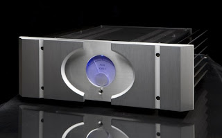
Home theater experts recommends that if the room is quite small, all you need for your home theater design is a television set, three speakers and a DVD player. The home theater design may be dependent of the shpre of the room; however, the position of the speakers remains to be the left, the right and the center of the room. Basic home theater design may require a television set bigger than 27 inches. Too small screen for your home theater design may not be sufficient for a movie theater-like experience. 

This is because even for the home theater design, you may need to consider the sight and sound of a movie theater. It is the main consideration why people go to a movie theater, the big screen and the surround sound. With respect to the surround sound of a movie theater, the basic three speakers is only applicable for smaller rooms, if the room is bigger, the home theater design needs to be more than three, you may go up to six speakers and a complimenting subwoofer may be necessary for the surround effect. Going back to a small room, if you will only put three speakers, you may want to consider buying a high quality brand speaker; this will give you enough surround sound for a smaller room. 

If you have a small budget, ensure that the store where you will buy your speakers will allow you to test the product in your room and if it will not give you a good surround sound, they should allow you to return or replace the unit. This is because some speakers sound good in the store but when you finally set them up in a small room, the effect is not very good. Find a neat deal where they can allow you to return or replace the speakers. However, if your budget is sufficient, you may consider hiring the services of a home theater designer. 

Your home theater designer will be able to design the home theater better and with complete accessories. He may require checking the power rating, and the need for amplifiers. He may also recommend using home theater projectors and he may recommend how the speakers need to be. You will get a good home theater design if you will be able to hire home theater designers. The need for home theater seating and television cabinet may also be necessary for the complete package of your home theater.

You may enjoy the entertainment without having to tide traffic jam and enjoy in your own home theater system. 

[Continue Reading]

2 way Active Crossover

Therefore this architecture represents the simplest access I could booty and still get the adapted outcome.The band akin audio arresting enters the absorber area it is astern out of phase.This is to atone for the filters which will alter the appearance afresh appropriately abiding the arresting to it’s able phase. The filters are more-or-less accepted low and aerial canyon filters appropriately however, added capacitors and resistors accept been added in adjustment to get the altruism bottomward to a minimum appliance alone E12 components.


This alive Cantankerous over is adequately beeline forward. It consists of a absorber and two 3rd order, 18 dB per octave filters. One low canyon and the added high. The cantankerous over abundance is set at 2Khz and is advised for AEK’s 400watt per access PA/Keyboard Amp systems. Obviously alone one access is apparent here.

This ambit may not be of awfully abundant use to anyone as it was accurately advised to clothing the applications. It is not capricious or switchable for two reasons. Firstly, it didn’t charge to be back the backdrop of the apostle arrangement were already known. And secondly, the added complication was put into the accurateness of the crossover rather than it’s flexibility. The filters are akin in account to anniversary added as able-bodied as can be accepted appliance alone E12 components. If switching were to be active to accord a ambit of abundance options, a accommodation would accept to be fabricated on clarify accuracy.

The alone added way to accomplish a accepted crossover architecture and advance accurateness would apparently be to use Switched capacitor clarify architecture blocks. In theory, two 18or 24dB per octave filters could be complete such that they tracked anniversary added by actuality bound to the aforementioned clock. This would be a nice agreement but I haven’t had the befalling to prove this technology for this affectionate of application. My primary affair was the breach through of switching babble appliance such a design.
[Continue Reading]

Power supply with driver TEA1507

Power supply with driver TEA1507 is mostly used by TV branded PHILIPS. Power Supply has an efficiency rate of up to 90% - thus requiring less cooling, as well as stand-by power required is less than 1 watt.


Power Supply with TEA driver is equipped with a variety of surge protector that has a high reliability - not easily damaged if any part of a damaged power supply circuit and power transistor or FET heat is not easily damaged. Power supply circuits are dapatapat working on ac input voltage between 85 up to 275v. The way it works with the driver circuit power supply TEA 1507 is quite simple, so easy tracking of damage to the circuit.

Power supply with driver TEA1507

The picture above is the basic power supply circuit with TEA1507
[Continue Reading]

LM139 Measure delay generator

Measure delay generator (in addition identified in the same way as sequence generator), is a device which long for provide output signals on prescribed time intervals from a time reference to and will unconsciously reset while the input hint returns to ground. under schematic illustrates the design of a measure Delay Generator Circuit Diagram using LM139. The LM139 skin tone from head to foot precision comparators; allows sensing come close to GND; eliminates need in lieu of dual food and power drain apt for battery setup.
 Delay Generator Circuit Diagram using LM139
 Delay Generator Circuit Diagram using LM139


[Continue Reading]

Rangkaian amplifier


Technical information

Datasheet IC 5G37
Vcc                = 6-12 V
Pout               = 0,4 W
RL                 = 8 Ohm
Ft                   = 40-17 Khz
Icco               = 15 mA
Package         = TABS1-14
Manufactered = China

[Continue Reading]

Thursday, November 21, 2013

Ultrasonic Wave Receiver Circuit

Ultrasonic Wave Receiver
Ultrasonic recipients will receive an ultrasonic signal emitted by an ultrasonic transmitter in accordance with the characteristic frequency. Received signal is going through the process of filtering using the frequency band pass filter circuit, with a frequency value that is passed has been determined.


Then the output signal will be amplified and passed to the comparator circuit (comparator) with a reference voltage determined based on the amplifier output voltage when the distance between the sensor mini vehicles with bulkhead / retaining walls to reach the minimum distance for the turn direction. Comparator output can be considered under these conditions is high (logic 1 ), while longer distances are low (logica0). Binary logics are then forwarded to the circuit controller (microcontroller).


The working principle of ultrasonic wave receiver circuit are as follows:

  • First - the first received signal will be strengthened first by the circuit transistor amplifier Q2.
  • Then the signal will be filtered using a high pass filter at a frequency of> 40kHz by a series of transistor Q1.
  • After the signal is amplified and filtered, then the signal will be rectified by diode D1 and D2 series.
  • Then the signal through a filter circuit low pass filter at a frequency <40kHz through the filter circuit C4 and R4.
  • After that the signal will go through the Op-Amp comparator U3.
  • So when there is an ultrasonic signal into the circuit, then the comparator will issue a logic low (0V), which will then be processed by the microcontroller to calculate the distance.
[Continue Reading]

Bridge Power Amplifier Using TDA7294

Using TDA7294 audio amplifier integrated circuit in bridge mode configuration , can be designed another Hi-Fi power amplifier .In this TDA7294 bridge power amplifier the value of the load must not be lower than 8 Ohm for dissipation and current capability reasons.

Bridge Power Amplifier Circuit Using TDA7294


The main advantages offered by TDA7294 bridge mode configuration are:High power performances with limited supply voltage level, Considerably high output power even with high load values ( 16 Ohm).The output power of this amplifier in bridge connection is 150 W with Rl= 8 Ohm , Vs = +/-25V the and 170 W output power for Rl=16 Ohm, Vs = +/-35V.
[Continue Reading]

Hybrid Headphone Amplifier

Potentially,
headphone listening can be technically superior since room reflections
are eliminated and the intimate contact between transducer and ear
mean that only tiny amounts of power are required. The small power
requirement means that transducers can be operated at a small fraction
of their full excursion capabilities thus reducing THD and other
non-linear distortions. This design of a dedicated headphones amplifier
is potentially controversial in that it has unity voltage gain and
employs valves and transistors in the same design.

Normal
headphones have an impedance of 32R per channel. The usual standard line
output of 775 mV to which all quality equipment aspires will generate a
power of U2 / R = 0.7752 / 32 = 18 mW per channel across a headphone
of this impedance. An examination of available headphones at well known
high street emporiums revealed that the sensitivity varied from 96 dB
to 103db/mW! So, in practice the circuit will only require unity gain
to reach deafening levels. As a unity gain design is required it is
quite possible to employ a low distortion output stage.

The
obvious choice is an emitter follower. This has nearly unity gain
combined with a large amount of local feedback. Unfortunately the
output impedance of an emitter follower is dependent upon the source
impedance. With a volume control, or even with different signal sources
this will vary and could produce small but audible changes in sound
quality. To prevent this, the output stage is driven by a cathode
follower,based around an ECC82 valve (US equivalent: 12AU7).

This
device, as opposed to a transistor configuration, enables the output
stage to be driven with a constant value, low impedance. In other
words, the signal from the low impedance point is used to drive the
high impedance of the output stage, a situation which promotes low
overall THD. At the modest output powers required of the circuit, the
only sensible choice is a Class A circuit. In this case the much
vaunted single-ended output stage is employed and that comprises of T3
and constant current source T1-T2.


Hybrid Headphone Amplifier circuit schematic

The
constant current is set by the Vbe voltage of T1 applied across R5
With its value of 22R, the current is set at 27 mA. T3 is used in the
emitter follower mode with high input impedance and low output
impedance. Indeed the main problem of using a valve at low voltages is
that it’s fairly difficult to get any real current drain. In order to
prevent distortion the output stage shouldn’t be allowed to load the
valve. This is down to the choice of output device. A BC517 is used for
T3 because of its high current gain, 30,000 at 2 mA! Since we have a
low impedance output stage, the load may be capacitively coupled via
C4.

Some purists may baulk at the idea of using an electrolytic
for this job but he fact remains that distortion generated by
capacitive coupling is at least two orders of magnitude lower than
transformer coupling. The rest of the circuitry is used to condition
the various voltages used by the circuit. In order to obtain a linear
output the valve grid needs to be biased at half the supply voltage.
This is the function of the voltage divider R4 and R2. Input signals
are coupled into the circuit via C1 and R1.

R1, connected
between the voltage divider and V1’s grid defines the input impedance
of the circuit. C1 has sufficiently large a value to ensure response
down to 2 Hz. Although the circuit does a good job of rejecting line
noise on its own due to the high impedance of V1’s anode and T3’s
collector current, it needs a little help to obtain a silent background
in the absence of signal. The ‘help’ is in the form of the capacitance
multiplier circuit built around T5. Another BC517 is used here to
avoid loading of the filter comprising R7 and C5. In principle the
capacitance of C5 is multiplied by the gain of T5.

In practice
the smooth dc applied to T5’s base appears at low impedance at its
emitter. An important added advantage is that the supply voltage is
applied slowly on powering up. This is of course due to the time taken
to fully charge C5 via R7. No trace of hum or ripple can be seen here on
the ‘scope. C2 is used to ensure stability at RF. The DC supply is
also used to run the valve heater. The ECC82 has an advantage here in
that its heater can be connected for operate from 12.6 V.

To run
it T4 is used as a series pass element. Base voltage is obtained from
the emitter of T5. T4 has very low output impedance, about 160 mR and
this helps to prevent extraneous signals being picked up from the
heater wiring. Connecting the transistor base to C5 also lets the valve
heater warm up gently. A couple of volts only are lost across T4 and
although the device runs warm it doesn’t require a heat-sink.
[Continue Reading]

Wednesday, November 20, 2013

Low Current Relay

Low current relay
This low current relay circuit is designed to be used in battery operated electronic devices. Its operating current is in micro amperes (µA). This is done by using a bistable relay and adding some components to force the relay to behave like a monostable relay.


A bistable relay stays at its last state when the power is turned off but consume at least 50mA trigger current. A monostable relay switches back to its original state when the power is turned off.
Low Current Relay


How does the low current relay works?

When the power is turned ON, the C1 charges via D1 and the relay coil and this current activates the relay. D1 ensures that the base of T1 is always more positive than its emitter and because of this T1 and T2 are always blocked.

Once the power is turned OFF, the emitter of T1 is coupled to the charge voltage at the positive pole of C1. Its base and the relay coil on the other hand are coupled to the negative pole of C1 and now T1 and T2 conduct, C1 can discharge through T2 and relay. The current flows to the relay coil but in reverse order so is activated to its other state.

It has the advantage of consuming little current, around 150 µA. For a reliable operation, select the relay’s operating voltage as 2/3 to 3/4 of the main power supply. For example is using a 12V power supply select a 9V relay.

Transistors replacements:
T1 = 2SA499 = BC557, BC558
T2 = 2SC734 = BC547, BC548
Low current relay switch

source:http://electroschematics.com/6546/low-current-relay/ 
[Continue Reading]

3V to 40 Volt DC Converter Circuit

Switching regulator subsystems intended for use as dc to dc converters. 3V to 40 Volt DC Converter circuit | The use of switching regulators is becoming more pronounced over that of linear regulators because the size reductions in new equipment designs require greater conversion efficiency. Another major advantage of the switching regulator is that it has increasednapplication flexibility of output voltage. The output can be less than, greater than, or of opposite polarity to that of the input voltage.

3V to 40 Volt DC Converter Circuit

Switching regulator subsystems intended for use as dc to dc converters. 3V to 40 Volt DC Converter circuit

The MC34063 series is a monolithic control circuit containing all the active functions required for dc to dc converters. This device contains an internal temperature compensated reference, comparator, controlled duty cycle oscillator with an active peak current limit circuit, driver, and a high current output switch. This series was specifically designed to be incorporated in step–up, step–down and voltage–inverting converter applications. These functions are contained in an 8–pin dual in–line package.

FEATURES 3V to 40 Volt DC Converter :
· Wide Input Voltage Range 3 V to 40 V
· Precision Internal Reference 2%
· High Output Switch Current Up to 1.5 A
· Short-Circuit Current Limiting
· Adjustable Output Voltage
· Low Standby Current
· Oscillator Frequency Up to 100 kHz
[Continue Reading]

Automatic Emergency Lamp Circuit

This is an automatic emergency lamp with day light sensing, means it senses darkness/night and turns ON automatically. Similarly it senses day light and turns OFF automatically. A simple emergency lamp which does not require any special equipment; even a multimeter to assemble and use. Any individual who can do a good quality soldering must be able to build this circuit successfully.

This can be easily accommodated in the defunct two 6 watt tube National Emergency Lamp or any PL tube type emergency lamp. The difference will be in the working; it will work non stop for more than 8 hours. Deep discharge is taken care by the LED characteristic and over charge protection is taken care by the fixed voltage regulator.This uses a simple 3Pin fixed regulator which has a built in current limiting circuit.

Simple Emergency Light Circuit Diagram: 

Automatic Emergency Lamp Circuit
The only required adjustment is the preset which has to be set to ensure the LEDs just light up (it should be left at that position). The 5mm LDR is just mounted on top of the emergency light as shown in the photograph. LDR is used to avoid it lighting up during day time or when the room lights are ON. 2 LEDs are used in series; the dropping resistance is avoided and 2 LEDs light up with current that is required for a single LED,  by which energy is saved to a great extent.

This particular circuit has been kept so simple for people who has limited access to components or in other words this is an emergency light that you can build with minimum components. In addition to circuit diagram, He has shared photographs of the prototype he made in National emergency light and a PCB design.
[Continue Reading]

Tuesday, November 19, 2013

Simple Stabilizer Circuit Diagram

Simple Stabilizer Circuit DiagramSimple Stabilizer Circuit Diagram

A aerial affection ability accumulation with a continuously capricious stabilised achievement adjustable at any amount amid 0 and 30VDC. The ambit additionally incorporates an cyberbanking achievement accepted limiter that finer controls the achievement accepted from a few milliamperes (2 mA) to the best achievement of three amperes that the ambit can deliver.

This affection makes this ability accumulation basal in the experimenters class as it is accessible to absolute the accepted to the archetypal best that a ambit beneath analysis may require, and ability it up then, after any abhorrence that it may be damaged if article goes wrong. There is additionally a beheld adumbration that the accepted limiter is in operation so that you can see at a glance that your ambit is beyond or not its preset limits.

[Continue Reading]

Hall Effect Sensors Magnetic Field

General picture of Hall Effect Sensors Magnetic Field Sensors as Hall effect sensor is a sensor used to detect the magnetic field.
Hall Effect sensor will produce a voltage proportional to the magnetic field strength received by a Hall effect sensor tersebut.Sensor it only consists of a silicon layer and two electrodes on each side of the silicon. By the time without any influence of the magnetic field then the potential difference between the two electrodes is 0 Volt as an electric current flowing in the middle two electrodes. When there is a magnetic field affecting the sensor is the current that flows will turn close to / away from the side that is affected by magnetic fields. This results in a potential difference between the two electrodes of Hall effect sensors, where the potential difference is proportional to the magnetic field received by the hall effect sensor.

Hall Effect Sensor Type UGN3503U
One example is a sensor hall effect sensor UGN3503U. UGN3503U sensor will produce a voltage proportional to the strength of the magnetic field detected by the sensor UGN3503U. UGN3503 sensor has 3 pins, namely:
Hall Effect Sensor Block Diagram UGN3503U

Hall Effect Sensor Type UGN3503U

Pin 1: VCC, supply voltage pin
Pin 2: GND, pin grounded
Pin 3: Vout, the output voltage pin.

In this sensor already built an amplifier that strengthens the signal from the sensor circuit and produce the output voltage in the middle of the supply voltage. In this sensor if it gets the influence of magnetic field polarity of the north pole it would result in a reduction in the output voltage on the contrary, if there is the influence of magnetic field polarity of the south pole it will result in an increase in the output voltage. This sensor can respond to changes in magnetic field strength from a static magnetic field strength and the strength of the magnetic field varies with frequency up to 20kHz.
UGN3503 hall effect sensor has a wide supply voltage is from 4.5V to 6V to the sensitivity of changes in magnetic field strength up to 23KHz frequency. The core of this system is the sensor UGN3503U. This sensor will produce output voltage 3V in the absence of magnetic field influence on the sensor. Tegagnan output is not strong enough so that it still needed an op amp is used to amplify the signal from the sensor changes UGN3503U.
[Continue Reading]

Battery Charger using LM317 Regulator

Battery Charger using LM317 Regulator

This Battery Charger is very similar to the universal charger that uses the constant current load. But this is much simpler to build and can be built using only two parties, the LM317 regulator and resistance. The use of diode D is for protection against short circuits. Capacitors C1 and C2 is good voltage regulation. Resistance R2 operates a dummy load when the battery is disconnected. The idea of ​​this magazine is the output current is equal to 1.2 V, divided by the value of R1.

Part List:
LM317
R1 - see the values in table below
R2 - 2.2 kilo-ohms 1/4W
C1,C2 - 47uF/25V, or any value will do, the higher the better
D - 1N4001 or any similar diode at-least 1A rated
[Continue Reading]

Simple Metal Detector Using 555 Timer

This metal detector electronic project schematic circuit is designed using a simple 555 timer integrated circuit . As you can see in the schematic circuit , this metal detector electronic project requires few external electronic parts . This circuit detects metal and also magnets.

Metal Detector with 555 Timer Circuit Daigram


When a magnet is brought close to the 10mH choke, the output frequency changes. This metal detector project can be powered from a power supply that can provide an output DC voltage between 6 an 12 volt . If a metal is closer to the L1 coil , will produce a change of output oscillation frequency, that will generate a sound in the 8 ohms speaker
[Continue Reading]

Monday, November 18, 2013

Hearing aids circuit

Hearing aids circuitCommercially available hearing aids are expensive. Here is a cheap hearing aid circuit that uses only four transistors and some passive components. In moving the power switch S to on position, the condenser microphone detects the sound signal, which is amplified by transistor T1 and T2.

Hearing aids circuit schematics
Now the amplified signal through coupling capacitor C3 to the basic Transistor T3. Signal further amplified by T4 to a PNP transistor drive low impedance earphones. Capacitors C4 and C5 is the power supply decoupling capacitor. This circuit can be easily installed in small, general purpose PCB or Vero board. It operates off of DC supply of 3V. For this, You can use two small 1.5V cells. Continue to switch S to the state off when circuit is not used. To increase the sensitivity of the condenser microphone, the house in a small tube. This fee circuit around Rs 65.
[Continue Reading]

Fire Sensor Hamamatsu UVTRON

Fire Sensor (Hamamatsu UVTRON)
UVTRON Hamamatsu R2868 is a sensor that detects a flame fire that emit ultraviolet light. Ultraviolet light emitted from a candle flame is a 5 meter can be detected by this sensor. This sensor can also detect some unseen phenomena such as high voltage transmission.


In order for this UVTRON sensors to connect to the system microcontroller then required a series of lawyer-signal condition that serves to change the response of UVTRON into pulses that can be recognized by the system microcontroller. With Module C3704 UVTRON response will then be processed into about 10 pulses mS and the maximum current 100mA. The output module uses the open configuration collector.
[Continue Reading]

100W BTL TDA2030 amplifier circuit

TDA2030 amplifier circuit using the BTL system has a 100W output power and voltage of +15 V,-15V 0. Amplifier circuit you can see below.

100W BTL TDA2030 amplifier circuit
TDA2030 100W amplifier circuit
Click image above to view larger.
[Continue Reading]

Sunday, November 17, 2013

Mini 2x75W Stereo Power Amplifier

Your search for audio power amplifier with 75W stereo power with a slim body, you can use this  Pyle - Mini 2x75W Stereo Power Amplifier - PCA3 . Power amp is designed simply and easily be placed anywhere, not just a good amplifier design is also very good in terms of sound quality in its gain. You can use this amplifier with a media player with a voice like VCD, DVD, Tape, etc.. What are you waiting you can buy the amplifier via the link below :
Pyle - Mini 2x75W Stereo Power Amplifier - PCA3
[Continue Reading]

Stereo Low power audio amplifier

Stereo Low power audio amplifier
Audio amplifier circuit has a power output of 2 x 2.3 Watt, which uses IC KA2206, KA22061, LA4180, LA4182, LA4183, LA4550, LA4555, LA4558. The required voltage for at least 6 volts to 13 volts DC maximum. Component takes is a ic that I mentioned above one of them, and several capacitors elco.


This Schematics low power amplifier

schematics LA4558

Component Description
C1 = 1uF
C2 = 100uF
C3 = 100uF
C4 = 100uF
C5 = 0.1uF
C6 = 470uF
C7 = 1uF
C8 = 100uF
C9 = 100uF
C10 = 100uF
C11 = 0.1uF
C12 = 470uF
ICs can use the ic which I mention above for each ic datasheet can be seen itself.
[Continue Reading]

Create a electric shock resistant tool

Youve electric shock?? .. Well, .. it was nice to recover all your gout! Sometimes true .. but we often do not touch circuit accidentally in the work that is still connected with line / grid (pln) .. pissed, wants I think we stepped on the stuff ..! patient first. 


Is there any easy way to avoid electric shock in repair work .. can even avoid the occurrence of ESD, if we deal with electronic goods which are sensitive to ESD (PC motherboards, mobile phones, circuit digital etc). you raft just like this series .. used as supply for the solder, when dealing with components which are sensitive to ESD and touch (CMOS IC). the greater capacity of the transformer Ampere. the greater the (good) power which can be handled. The second transformer is identical / similar.
[Continue Reading]

Saturday, November 16, 2013

Volume Controller Equalizer Using LM1036

This volume controller equalizer electronic project is designed using LM1036 DC tone volume controller with volume and balance circuit for stereo applications .An additional control input of the LM1036 allows loudness compensation to be simply effected.

Volume Controller Equalizer Circuit Using LM1036


The four control inputs of the LM1036 volume controller provides control of the bass, treble, balance and volume functions through application of DC voltages from a remote control system or, alternatively, from four potentiometers which may be biased from a zenner regulated supply provided on the circuit.Each tone response is defined by a single capacitor chosen to give the desired characteristic.
[Continue Reading]